Opto-line is dedicated to the highest quality custom optical patterns and coatings
About Opto-Line International
Industry leaders in the manufacturing of precision reticles
History: Since 1967, Opto-Line International has built a reputation for excellence, providing companies in the medical, optometry, aerospace, industrial, science and defense sectors with the very best custom precision optical patterns and thin film coatings available. Opto-Line International’s expertise in photolithography, combined with our thin film coating capability, enables us to provide our customers with the finest precision patterned optics…often the most complex and demanding.
Pattern Capabilities
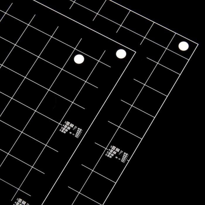
Using our customers’ specifications, drawings, CAD files, or simply their ideas, Opto-Line can replicate almost any custom pattern on various optics. Opto-Line’s minimum feature size is approximately 1μm or 500 line pairs per mm. Multiple patterns of different coating materials may be delineated on the same surface with precision alignment. Custom patterns on both surfaces with extremely accurate alignment from front to back surface are also possible.
Thin Film Coating Capabilities
The patterns Opto-Line delineates are typically coated in chrome, gold, aluminum, protected aluminum, Inconel, NiChrome, SiO, SiO2, MgF2, and our proprietary low-reflecting black chrome. Typical coating thicknesses range from 300 – 10,000 Angstroms.
Substrates Types
We pattern on a myriad of optical substrates including but not limited to all glass material [BK7, D260, soda lime, etc.], IR materials [germanium, silicon, zinc sulfide, quartz, sapphire, zinc selenide], ceramics, Mylar and Kapton and others.
Substrate Size
The largest substrate size that Opto-Line can pattern is approximately 12.5” diagonal.
The smallest part we can pattern/manufacture is about 1mm x 1mm.
Photoresist Wafer Coatings
Opto-Line utilizes a semi-automated system in our class 100 clean room to coat wafers up to Ø300mm
Lenses
One specialty that separates Opto-Line from other companies is our ability to put precision patterns on lenses (concave, convex). Feasibility depends on the radius and the feature sizes.
Applications
Our custom precision optical patterns are used in thousands of products and systems throughout the world. Just a few applications for our patterning solutions include satellite navigation systems, endoscopes, optometry, modulated contrast microscope objectives, electro-optical devices, optical system calibration, photolithographic systems, surveillance systems, and microscopy.
Opto-Line International takes great pride in the high level of quality achieved during the manufacture of product at our facility.
Our 9800 sq ft facility includes a Class 100 clean room, multiple high-vacuum evaporation chambers, and modern equipment allowing us to process your custom requirements.
Cleanliness and careful handling of sensitive optical components is of paramount importance to every employee.
Unparalleled Service. Undeniable Quality.
Our team has over 160 combined years of service at Opto-Line International.
Treating our employees well and with respect directly translates to superior service and product.
Our blanket photoresist coatings for semiconductor test wafers are processed in a dedicated, class 100 cleanroom. Wafer sizes range from 50mm diameter to 300mm diameter. Coating thicknesses range from 0.5 microns to 10 microns.
Blanket photoresist coatings may also be patterned per customer specifications. Coating thickness and uniformity can be certified at the customers request.