by Opto-Line | Feb 27, 2020 | Company News, Custom Patterns
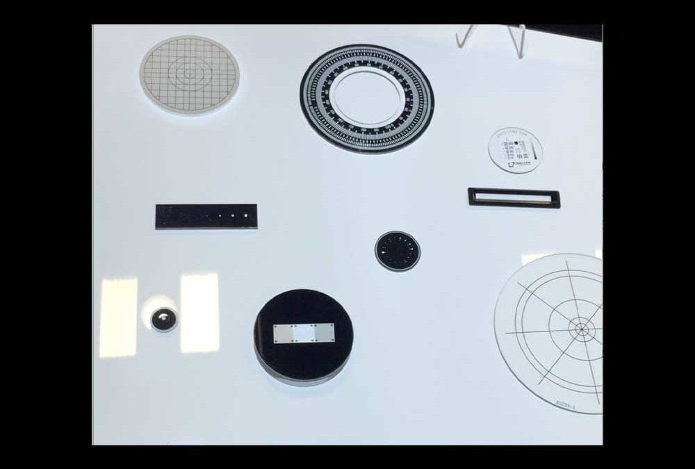
We are not your standard, stock reticle company. Instead, Opto-Line manufactures your unique, custom patterns on optical substrates per your requirements. Within our limitations of about 1μm, we can produce any pattern you may need with the precision and quality you...

by Opto-Line | Feb 25, 2020 | Aerospace, Company News, Custom Patterns
Opto-Line has provided various custom patterns typically utilizing our low-reflecting black chrome. For Aerospace applications, our precision pattern and coatings are often found in systems created by the most well-known companies. Many of our aerospace reticles are...
by Opto-Line | Feb 21, 2020 | Company News, Photoresist Coatings
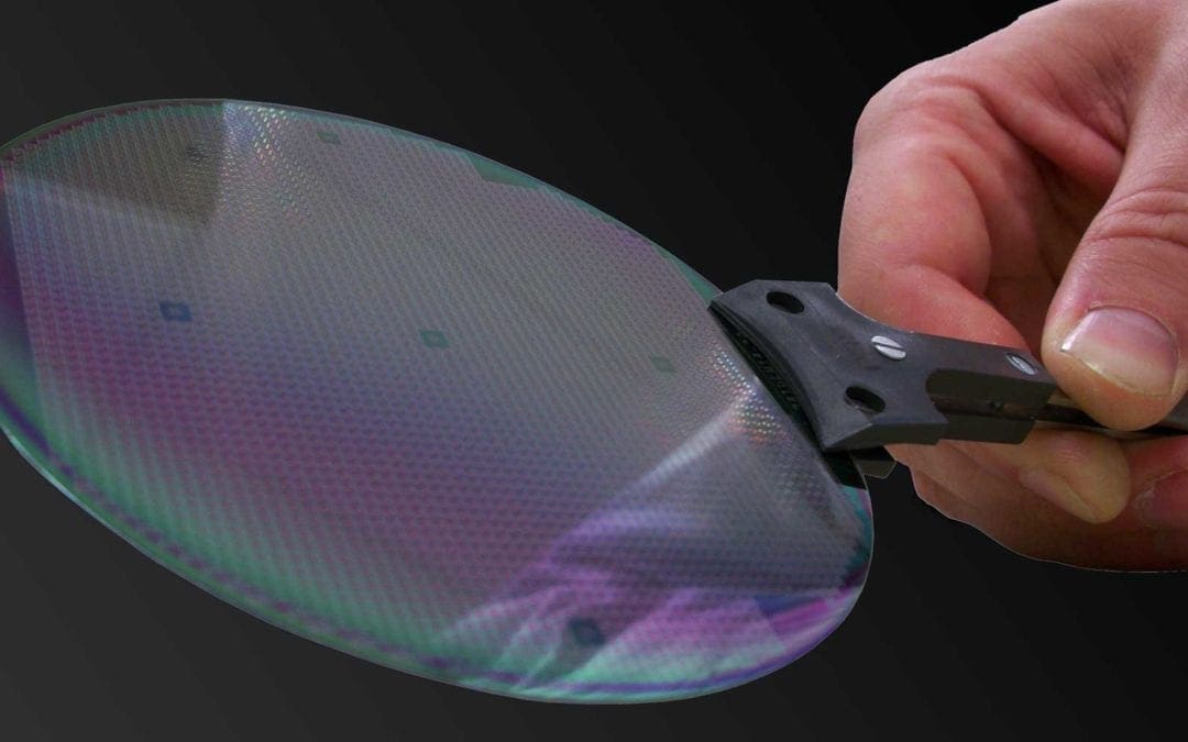
Experience and techniques that outshine the competition Whether it be silicon wafers that need a custom resist patterns, a 7” plate, or a Ø10mm concave optic, Opto-Line’s ability to provide photoresist patterns on a multitude of optics is just one factor that makes us...

by Opto-Line | Feb 3, 2020 | Custom Patterns, Photoresist Coatings
Wafer sizes range from 50mm diameter to 300mm diameter. Coating thicknesses range from 0.5 microns to 10 microns. A photoresist is a light-sensitive material used in several industrial processes, such as photolithography and photoengraving, to form a patterned coating...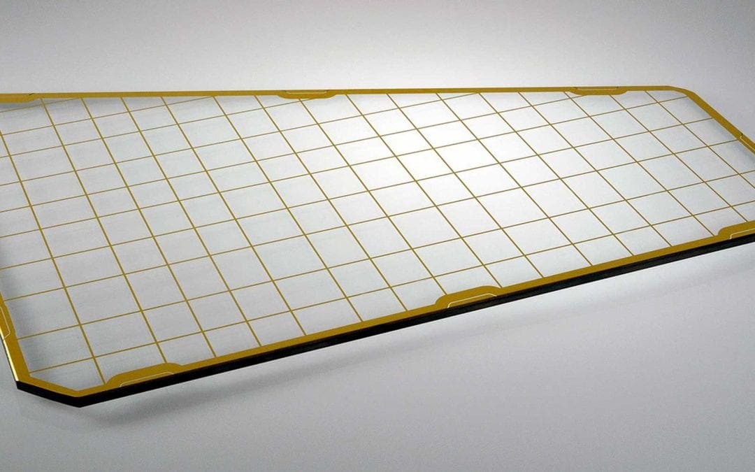

 Precision EMI Grids, Range Finder Reticles and Custom Patterned Optics