We Provide Custom Services and Solutions for your Precision Optical Pattern Needs We are here to answer your questions!
We Provide Custom Services and Solutions for your Precision Optical Pattern Needs We are here to answer your questions!

Custom patterned lenses for the Aerospace Industry Opto-Line has provided various custom patterns typically utilizing our low-reflecting black chrome. For Aerospace applications, our precision pattern and coatings are often found in systems created by the most well-known companies.
For more than 50 years, the Opto-Line name has been synonymous with the highest quality service. Opto-Line has a long history of partnering with many companies over the years to help them achieve their product goals. Often times our custom patterns are vital in the R&D phase of a product. Opto-Line’s ability to think out […]
Opto-Line provides Custom Precision Patterns and Photoresist Coatings to meet the specific needs of our clients. While our precision patterns are made via thin film coatings, we are not a coating house. Instead we focus and specialize in the custom patterning service our clients require on a wide array of optical substrates. Reticles are a […]
Your Specifications, Your Way. As industry leaders in the manufacturing of precision reticles, Opto-Line specializes in custom optical patterns and apertures with over 40 years of experience. We welcome projects that others are unwilling to tackle. Our customers are our #1 priority. “We are realizing things that Opto-Line can do for us that we never […]
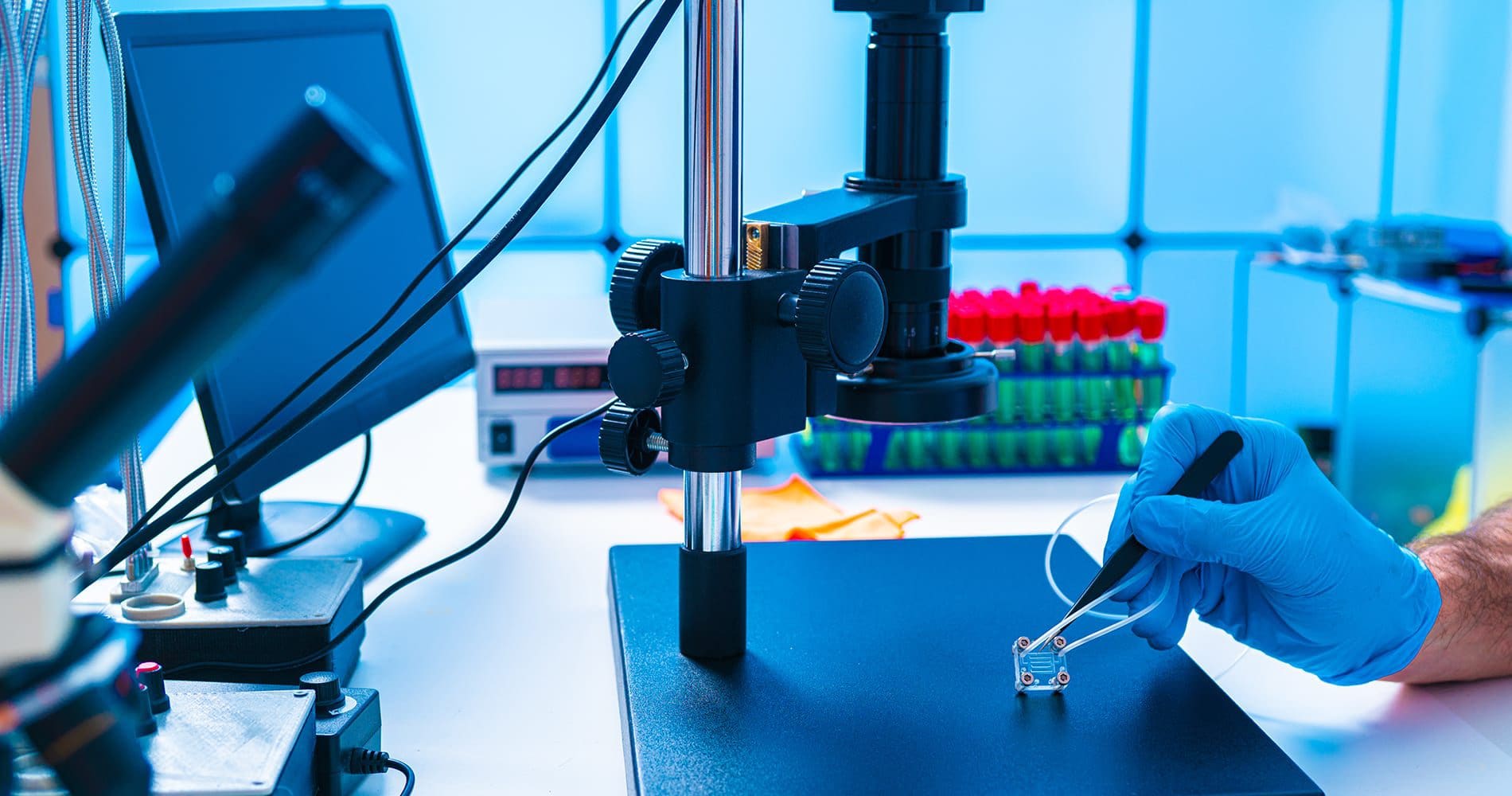
Photolithography, also termed optical lithography or UV lithography, is a process used in microfabrication to pattern parts of a thin film or the bulk of a substrate. Opto-Line offers the highest quality Blanket Photoresistor Coatings. By using a semi-automated photoresist coating system in a class 100 clean room, Opto-Line is able to provide its clients […]
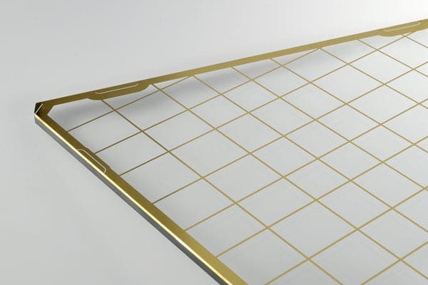
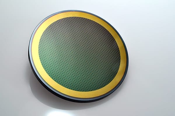
Using our customers’ specifications, drawings, CAD files, or simply their ideas, Opto-Line can replicate almost any custom pattern on various optics. Opto-Line’s minimum feature size is approximately 1μm or 500 line pairs per mm. Multiple patterns of different coating materials may be delineated on the same surface with precision alignment. Custom patterns on both surfaces […]
Since 1967, Opto-Line International has built a reputation for excellence, providing companies in the medical, optometry, aerospace, industrial, science and defense sectors with the very best custom precision optical patterns and thin film coatings available. Opto-Line International’s expertise in photolithography, combined with our thin film coating capability, enables us to provide our customers with the […]
Experience and techniques that outshine the competition Whether it be silicon wafers that need a custom resist patterns, a 7” plate, or a Ø10mm concave optic, Opto-Line’s ability to provide photoresist patterns on a multitude of optics is just one factor that makes us stand out. We have many customers that want to utilize their […]
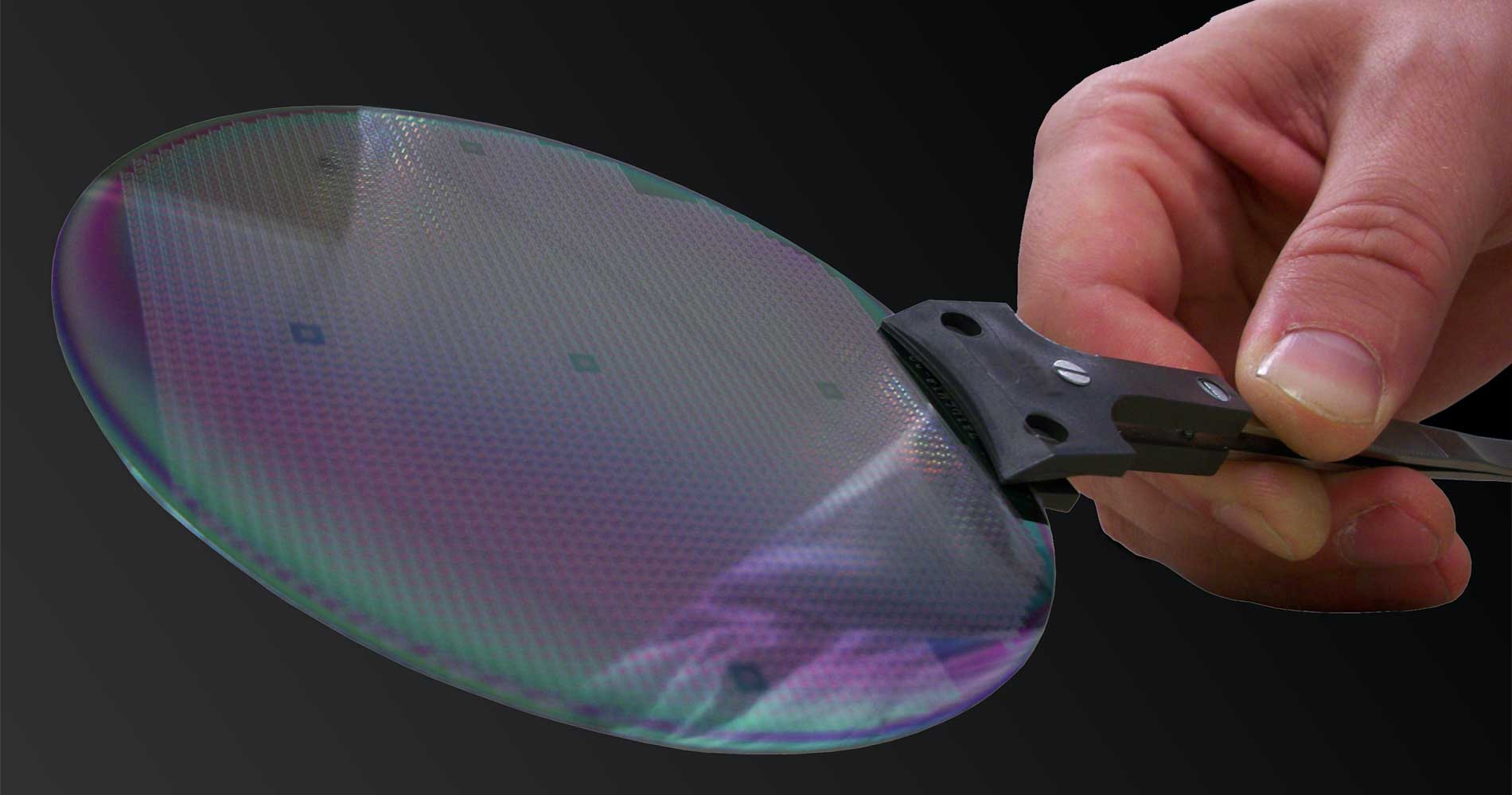
Wafer sizes range from 50mm diameter to 300mm diameter. Coating thicknesses range from 0.5 microns to 10 microns. A photoresist is a light-sensitive material used in several industrial processes, such as photolithography and photoengraving, to form a patterned coating on a surface. Blanket photoresist coatings may also be patterned per customer specifications. Coating thickness and […]
 What are custom precision optical patterns used for? Opto-Line is often asked this question but the answer is not so simple. The variety of markets and end products is almost endless…
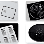 From 1951 USAF resolution test charts to almost any custom test targets imaginable, Opto-Line can produce any pattern you need with pinpoint precision and accuracy. Request a quote today for your test target needs.
 Opto-Line strives to perfect your patterned lens projects utilizing advanced skills and processing methods. Visit us online at opto-line.com to learn more or call us at (978) 658-7255.
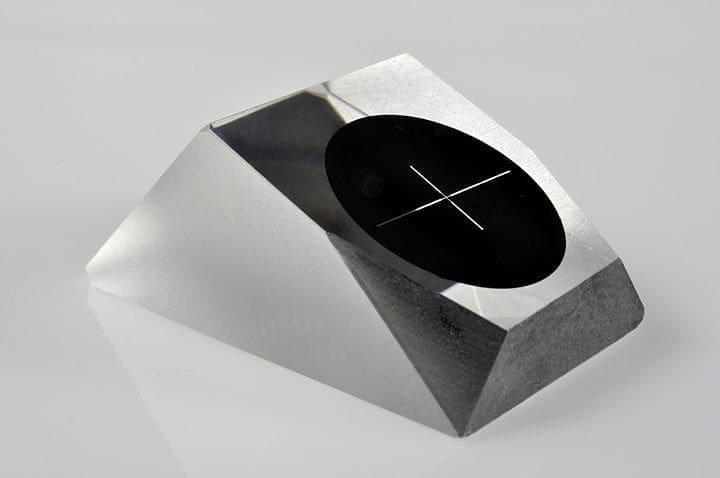
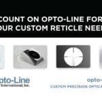 Opto-Line provides custom precision reticles for optical scopes and siting devices for a multitude of clients. The high level of quality achieved during the manufacturing of our custom reticles is a source of great pride. We invite you reach out to learn more – (978) 658-7255.
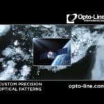 Many of our aerospace reticles are used in sun angle sensor systems on satellites. It is not only our dependable and time-tested coating that separates Opto-Line from other companies but the precision we can accomplish in the detailed patterns. Please contact us to find out how we can partner with you on your next project.