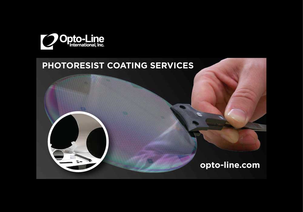
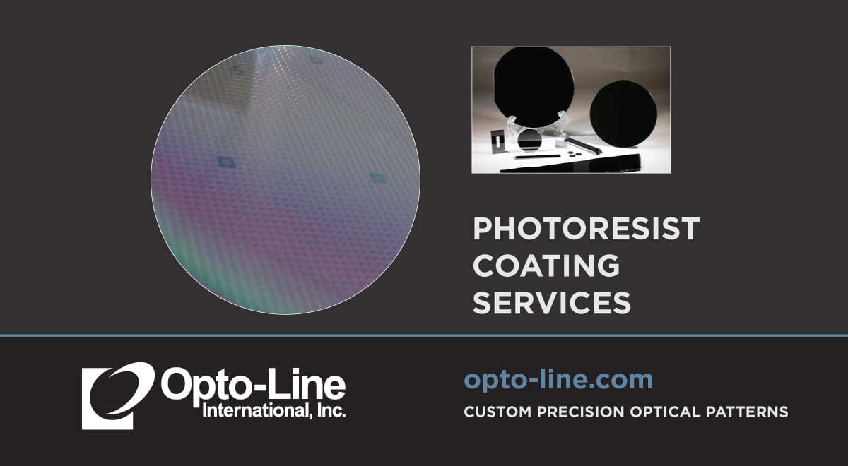
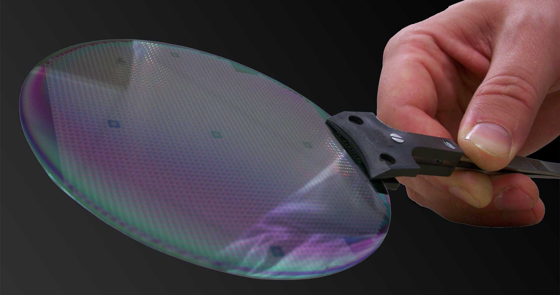
Opto-Line’s blanket photoresist coating services for semiconductor test wafers are processed in a dedicated, class 100 cleanroom. Wafer sizes range from 50mm diameter to 300mm diameter. Coating thicknesses range from 0.5 microns to 10 microns. A photoresist is a light-sensitive material used in several industrial processes, such as photolithography and photoengraving, to form a patterned […]

Opto-Line’s blanket photoresist coating services for semiconductor test wafers are processed in a dedicated, class 100 cleanroom. Wafer sizes range from 50mm diameter to 300mm diameter. Coating thicknesses range from 0.5 microns to 10 microns. A photoresist is a light-sensitive material used in several industrial processes, such as photolithography and photoengraving, to form a patterned […]
Wafer sizes range from 50mm diameter to 300mm diameter. Coating thicknesses range from 0.5 microns to 10 microns. A photoresist is a light-sensitive material used in several industrial processes, such as photolithography and photoengraving, to form a patterned coating on a surface. Blanket photoresist coatings may also be patterned per customer specifications. Coating thickness and […]

Wafer sizes range from 50mm diameter to 300mm diameter. Coating thicknesses range from 0.5 microns to 10 microns. A photoresist is a light-sensitive material used in several industrial processes, such as photolithography and photoengraving, to form a patterned coating on a surface. Blanket photoresist coatings may also be patterned per customer specifications. Coating thickness and […]