Opto-Line International has been creating custom precision patterns on optics since 1967 We are not your standard, stock reticle company. Instead, Opto-Line manufactures your unique, custom patterns on optical substrates per your requirements. From reticles and apertures to multi-density resolution masks and almost any pattern imaginable, our photolithography and thin film coatings practices are optimized […]

Just a few applications for our patterning solutions include satellite navigation systems, endoscopes, optometry, modulated contrast microscope objectives, electro-optical devices, optical system calibration, photolithographic systems, surveillance systems, and microscopy. Opto-Line International takes great pride in the high level of quality achieved during the manufacture of product at our facility. Our 9800 sq ft facility includes […]

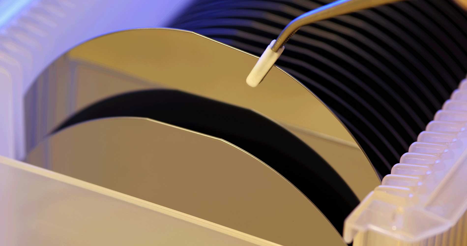
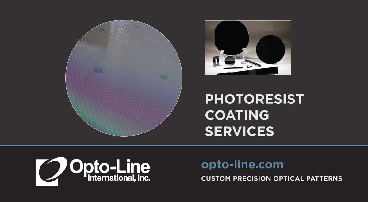
Opto-Line Offers a Variety of Options for your Photoresist Coating Needs Photolithography, also termed optical lithography or UV lithography, is a process used in microfabrication to pattern parts of a thin film or the bulk of a substrate. Opto-Line offers the highest quality Blanket Photoresistor Coatings. By using a semi-automated photoresist coating system in a […]

Opto-Line International, Inc. is a customer oriented small business that strives to provide outstanding quality and service. From a small order of one part to high volume needs, Opto-Line treats every job as critical and dedicates its resources, knowledge and skills to delivering exceptional reticles, apertures and precision patterns.

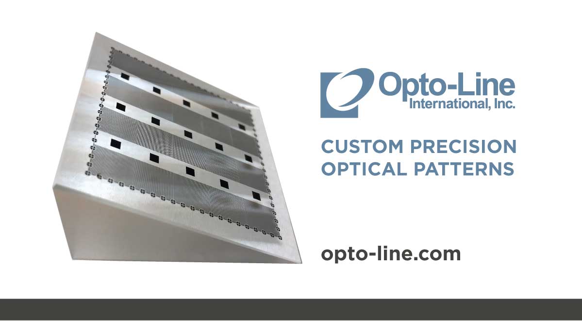
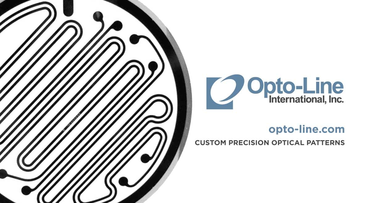
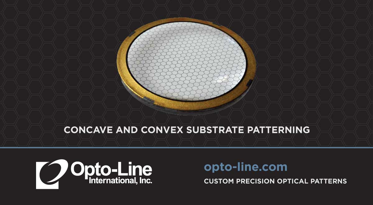
Typically one part of a larger component, our patterned optics are critical to our customers’ final product. Some examples of our custom patterning capabilities include reticles, resolution test targets, EMI grids, apertures, linear scales, and neutral density step tablets. Opto-Line can typically tackle any custom pattern imaginable. We are proud to deliver some of the […]

Opto-Line International’s expertise in photolithography, combined with our thin film coating capability, enables us to provide our customers with the finest precision patterned optics…often the most complex and demanding. We’d love to hear from you. Please tell us more about your custom optical pattern needs by completing the form below or calling us at (978) […]

Custom Precision Optical Patterns • Photoresist Coatings The Opto-Line name is synonymous with Service. It is our mission to provide you with the best service and quality. It is your satisfaction that has kept us in business for over fifty years.

Wafer sizes range from 50mm diameter to 300mm diameter. Coating thicknesses range from 0.5 microns to 10 microns. A photoresist is a light-sensitive material used in several industrial processes, such as photolithography and photoengraving, to form a patterned coating on a surface. Blanket photoresist coatings may also be patterned per customer specifications. Coating thickness and […]

Our photolithography techniques are done with the utmost care and precision. Our team has over 100 years of total experience resulting in a tried and true methodology for delineating your patterns. We invite you to learn more about how Opto-Line can meet your custom lens patterning needs. Visit our Precision Lens Pattern Services Page

Opto-Line International has been creating custom precision patterns on optics since 1967 We are not your standard, stock reticle company. Instead, Opto-Line manufactures your unique, custom patterns on optical substrates per your requirements. From reticles and apertures to multi-density resolution masks and almost any pattern imaginable, our photolithography and thin film coatings practices are optimized […]
