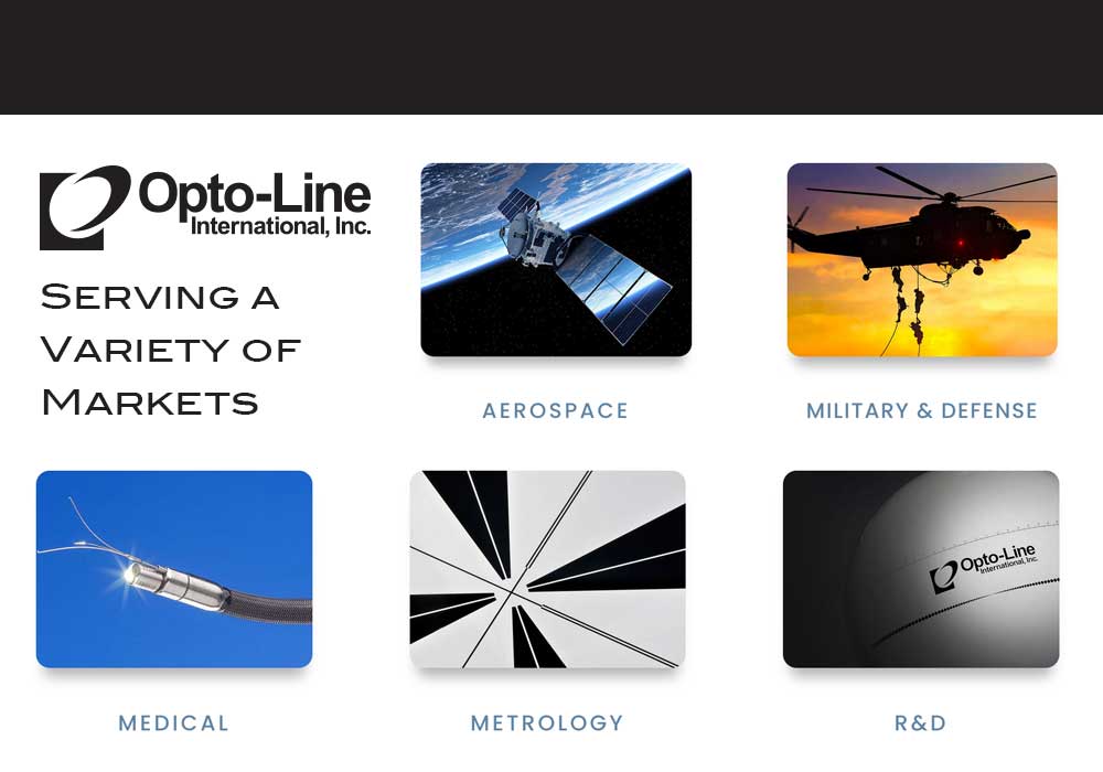
No matter the complexity, Opto-Line International has helped hundreds of clients across many markets from Aerospace to Clean Energy with their custom precision optical pattern and coating needs. To learn more about some of the markets we serve, we invite you to click the button below.

Since 1967, Opto-Line International has built a reputation for excellence, providing companies in the medical, optometry, aerospace, industrial, science and defense sectors with the very best custom precision optical patterns and thin film coatings available.

Opto-Line International’s expertise in photolithography, combined with our thin film coating capability, enables us to provide our customers with the finest precision patterned optics…often the most complex and demanding.

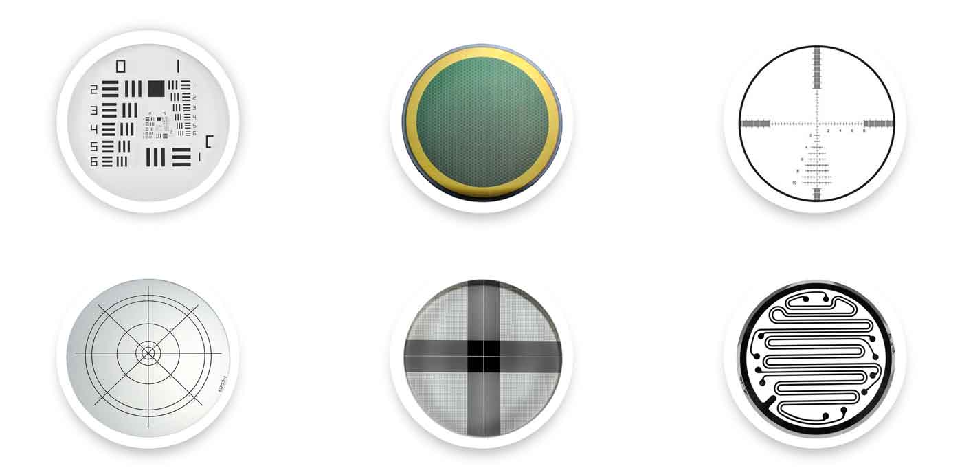
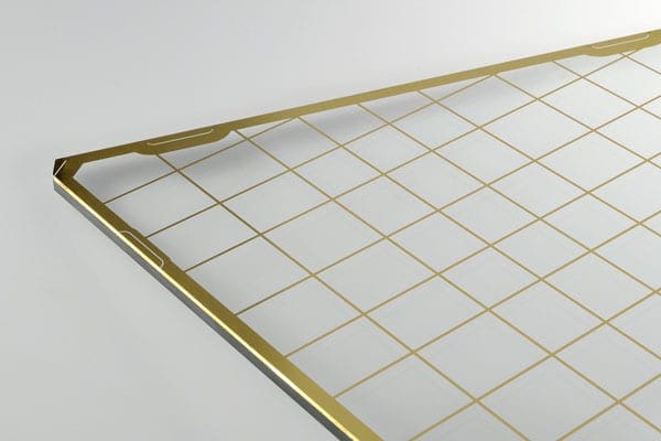
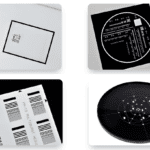
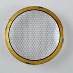
From reticles and apertures to multi-density resolution masks and almost any pattern imaginable, Opto-Line can produce your end-product on any of the following substrates types: Full spectrum of glass material IR materials [germanium, silicon, zinc sulfide, quartz, sapphire] Ceramics Stainless Steel Mylar Kapton

Photolithography, also termed optical lithography or UV lithography, is a process used in microfabrication to pattern parts of a thin film or the bulk of a substrate. Opto-Line offers the highest quality Blanket Photoresistor Coatings. By using a semi-automated photoresist coating system in a class 100 clean room, Opto-Line is able to provide its clients […]

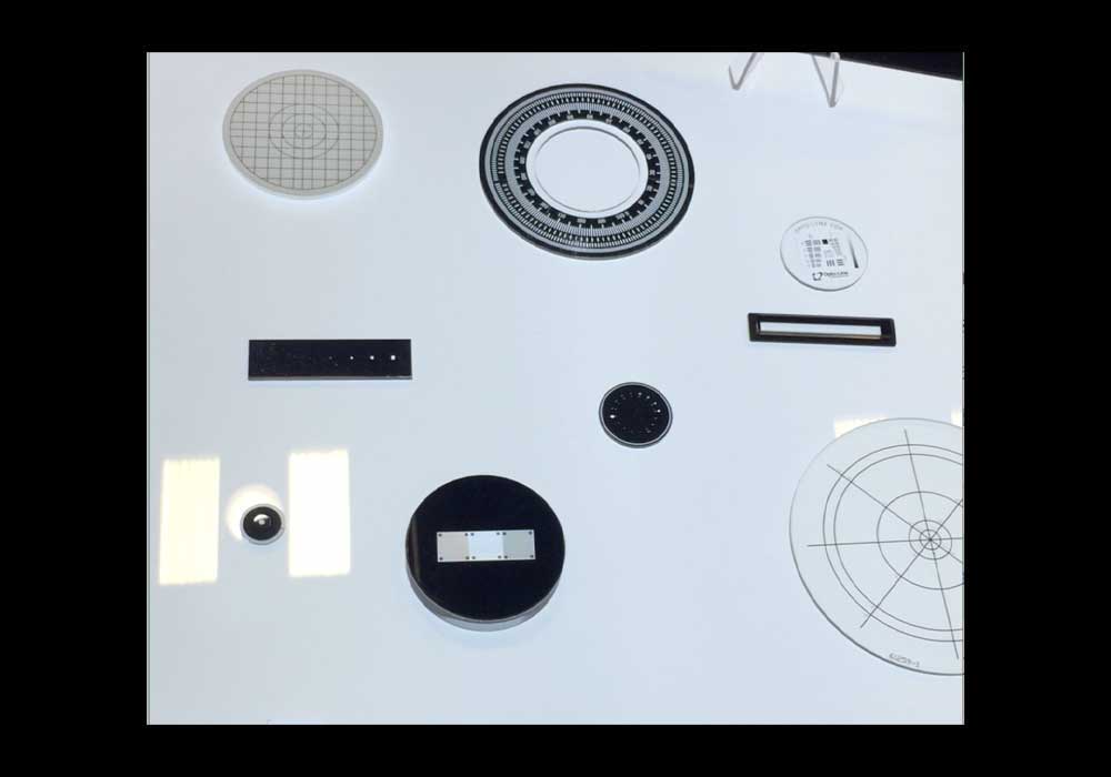
Using our customers’ specifications, drawings, CAD files, or simply their ideas, Opto-Line can replicate almost any custom pattern on various optics. Opto-Line’s minimum feature size is approximately 1μm or 500 line pairs per mm. Multiple patterns of different coating materials may be delineated on the same surface with precision alignment. Custom patterns on both surfaces […]

Since 1967, Opto-Line International has built a reputation for excellence, providing companies in the medical, optometry, aerospace, industrial, science and defense sectors with the very best custom precision optical patterns and thin film coatings available. Pattern Capabilities Using our customers’ specifications, drawings, CAD files, or simply their ideas, Opto-Line can replicate almost any custom pattern […]
Opto-Line offers custom patterning capabilities include reticles, resolution test targets, EMI grids, apertures, linear scales, and neutral density step tablets. We can typically tackle any custom pattern imaginable. Combined with our specialized photolithography, Opto-Line utilizes thin film coatings to make your custom patterns. Our high-vacuum evaporation chambers provide us with the ability to precisely deposit […]
Experience and techniques that outshine the competition Whether it be silicon wafers that need a custom resist patterns, a 7” plate, or a Ø10mm concave optic, Opto-Line’s ability to provide photoresist patterns on a multitude of optics is just one factor that makes us stand out. We have many customers that want to utilize their […]