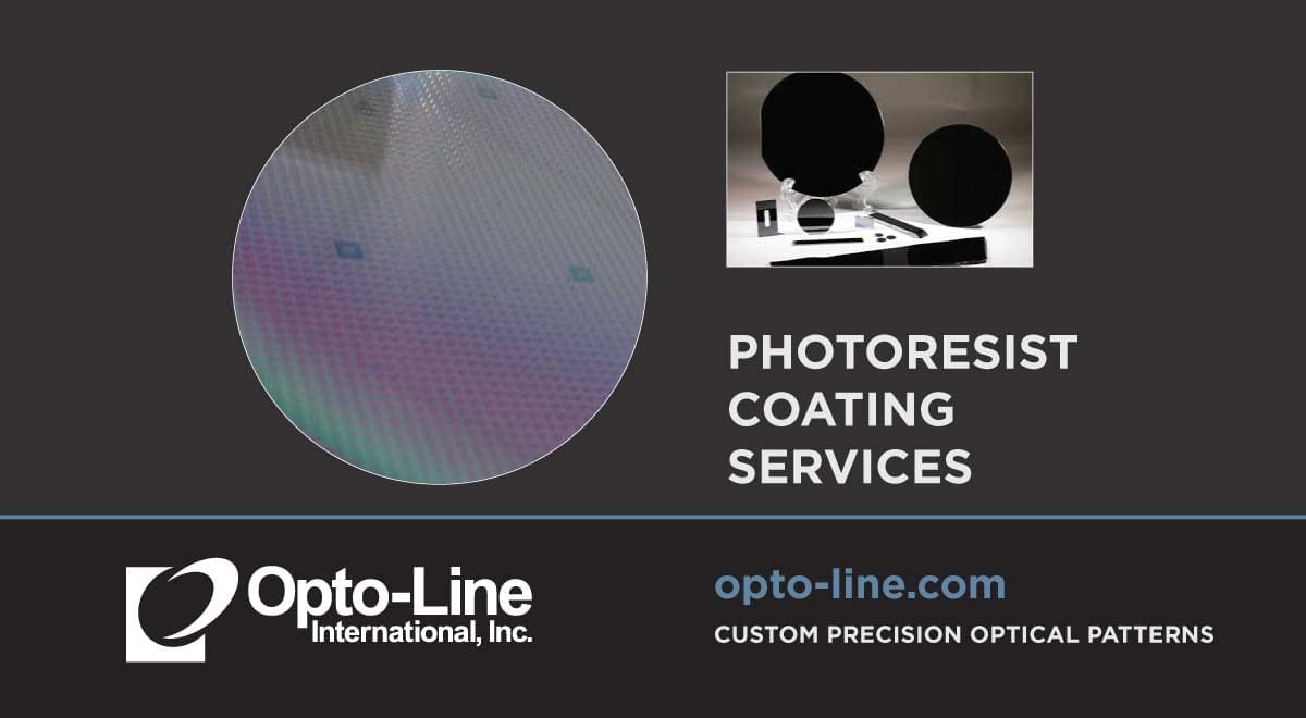
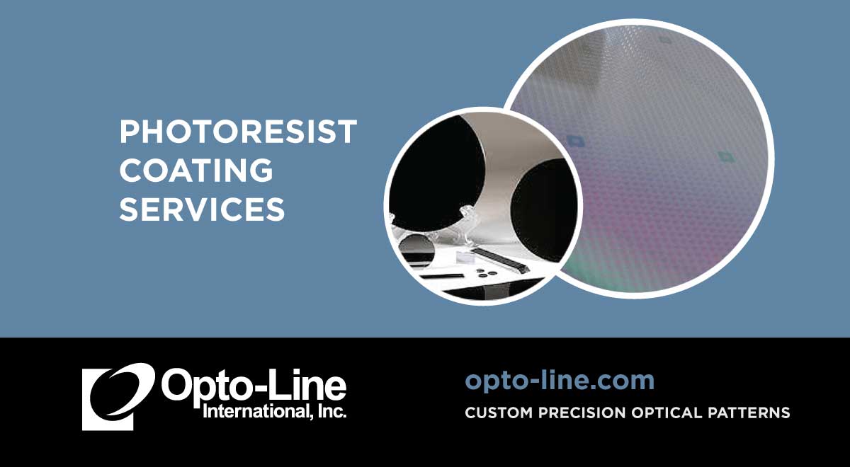
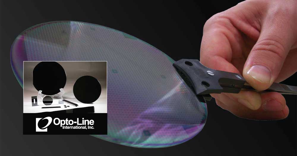
Whether it be silicon wafers that need custom resist patterns, a 7” plate, or a Ø10mm concave optic, Opto-Line’s ability to provide photoresist patterns on a multitude of optics is just one factor that makes us stand out. We have many customers that want to utilize their own coatings but do not have the ability […]

For over 50 years, the Opto-Line name has been synonymous with service. It is our mission to provide you with the best service and quality and it has been your satisfaction that has kept us in business all these years.

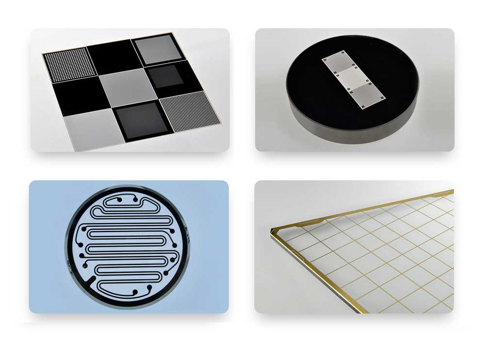
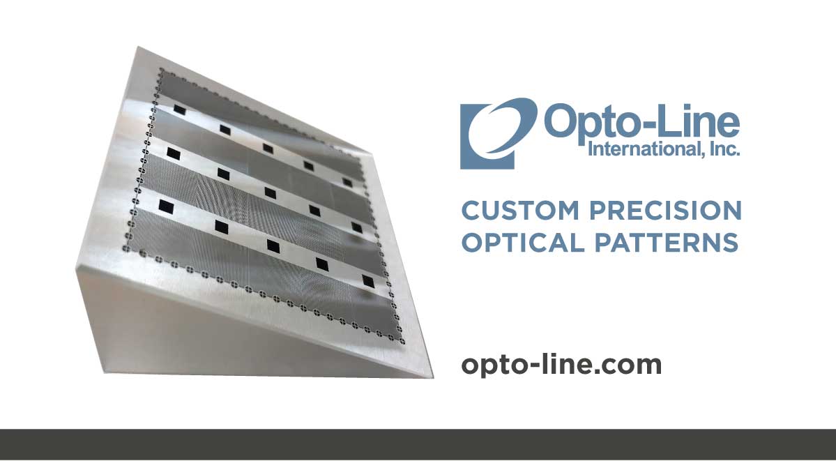
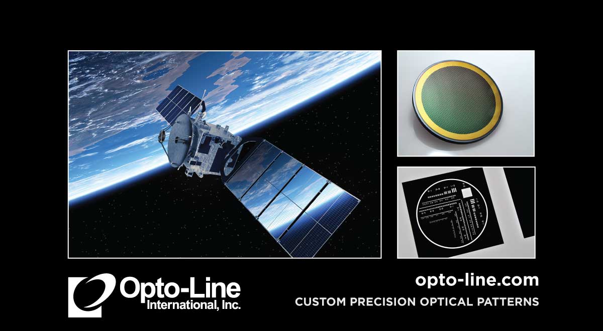
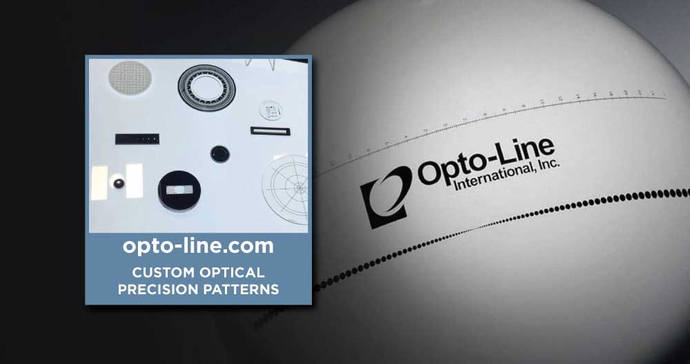
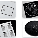
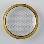
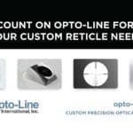
Combined with our specialized photolithography, Opto-Line utilizes thin film coatings to make your custom patterns. Some examples of our custom patterning capabilities include reticles, resolution test targets, EMI grids, apertures, linear scales, and neutral density step tablets. Opto-Line can typically tackle any custom pattern imaginable.

The Opto-Line name is synonymous with service. It is our mission to provide you with the best service and quality. It is your satisfaction that has kept us in business for over fifty years. Opto-Line International takes great pride in the high level of quality achieved during the manufacture of product at our 9800 sq […]

Whether it be silicon wafers that need a custom resist patterns, a 7” plate, or a Ø10mm concave optic, Opto-Line’s ability to provide photoresist patterns on a multitude of optics is just one factor that makes us stand out. We have many customers that want to utilize their own coatings but do not have the […]

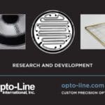
Cleanliness and the careful handling of sensitive optical components is of the highest importance for every employee. Opto-Line International takes tremendous pride in the high level of quality achieved during the manufacture of these products at our state of the art facility. Our modern equipment, including multiple high-vacuum evaporation chambers and a Class 100 clean […]

Some examples of our custom patterning capabilities include reticles, resolution test targets, EMI grids, apertures, linear scales, and neutral density step tablets. Opto-Line can typically tackle any custom pattern imaginable. We take great pride in the exceptional quality of our work and invite you to reach out today to learn more about how we can […]

Utilizing a semi-automated coating system allows us to provide our clients with an extremely quick lead time and a high quality coating. Please contact us so we can learn more about your custom optical pattern needs.

Combined with our specialized photolithography, Opto-Line utilizes thin film coatings to make your custom patterns. Some examples of our custom patterning capabilities include reticles, resolution test targets, EMI grids, apertures, linear scales, and neutral density step tablets. Opto-Line can typically tackle any custom pattern imaginable.

Our blanket photoresist coating services for semiconductor test wafers are processed in a dedicated, class 100 cleanroom. We’d love to hear from you. Please tell us more about your custom optical pattern needs.