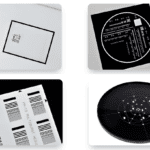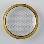
Specializing in custom precision optical patterns for all areas of research and development, Opto-Line helps clients reach their R&D goals. Our custom patterns are often vital components in the R&D phase of a product. We have a long history of partnering with companies across an array of industries to help them achieve their product goals. […]

Wafer sizes range from 50mm diameter to 300mm diameter. Coating thicknesses range from 0.5 microns to 10 microns. A photoresist is a light-sensitive material used in several industrial processes, such as photolithography and photoengraving, to form a patterned coating on a surface. Blanket photoresist coatings may also be patterned per customer specifications. Coating thickness and […]


